.png)
|
|
Logic Gates are the building blocks of digital circuits, taking binary values as input and returning a binary value as output after performing a logical operation. There are several kinds of gates available in Digital Electronics like basic gates, and universal gates. Implementation of the XOR gate from the NAND gate is possible because the NAND gate is a Universal gate i.e., it can implement all other gates. The NAND gate gives the output 0 if all the inputs are 1 else it gives 1 for all other cases. XOR gate is a logic gate that gives output 1 when several 1s are odd else it gives 0. In this article, we will explore the XOR gate, and NAND gate and implement the XOR gate from the NAND gate. Table of Content What is an XOR Gate?In digital electronics, the XOR (Exclusive-OR) Gate is a combination of all three fundamental or basic gates (NOT, AND and OR gates). It receives two or more than two input signals but produces only one output signal. It results in a low (0) if the input bit pattern contains an even number of high(1) signals. The output is high (1) for an odd number of high (1) signals in the input bit pattern. The XOR gate’s behavior can be summarized as follows
The Boolean expression of two input XOR Gate is as follows Say we have two inputs, A and B and the output is called X, then the expression is:
Logic Diagram of Two Input XOR GateThe logic circuit diagram of the XOR gate is shown in the following figure. It has two input line denoted by the letter A and B and one output line denoted by the letter X, where X=A⊕B= A’B+AB’. The Boolean expression of Three input XOR Gate is as follows 2 Input XOR Gate Truth Table of Two input XOR GateThe truth table of two input XOR gate is given below. This table shows the relationship between two inputs and one output of the XOR gate. This also provides information about the operation of XOR gate for different input combinations. Logic Diagram of Three Input XOR GateThe logic circuit diagram of the XOR gate is shown in the following figure. It has three input line denoted by the letter A, B, C and one output line denoted by the letter X, where X=A⊕B⊕C. The Boolean expression of N input XOR Gate is as follows: 3 Input XOR Gate Say we have N inputs, A0, A1, …., AN and the output is called X, then the expression is:
Truth Table of Three input XOR GateThe truth table of three input XOR gate is given below. This table shows the relationship between three inputs and one output of the XOR gate. This also provides information about the operation of XOR gate for different input combinations. Say we have three inputs, A, B and C and the output is called X, then the expression is:
Logic Diagram of N input XOR GateThe logic circuit diagram of the XOR gate is shown in the following figure. It has N input line denoted by the letter A0, A1, …., AN and one output line denoted by the letter X, where X=A0⊕A1⊕…..⊕AN.  N Input XOR Gate What is a NAND Gate?NAND Gate is a combination of AND and NOT Gate. In this gate, a NOT Gate is applied at the output of an AND Gate. It receives two or more than two input signals but results in only one output signal which is complement of product of all the input signals. This is the reason that a NAND Gate is also referred as complemented AND Gate or Inverted AND Gate. The NAND gate’s behavior can be summarized as follows
The Boolean expression of two input NAND Gate is as follows Say we have two inputs, A and B and the output is called X, then the expression is:
Truth Table of Two Input NAND GateThe truth table of two input NAND gate is given below. This table shows the relationship between two inputs and one output of the NAND gate. This also provides information about the operation of NAND gate for different input combinations. Logic Diagram of Two Input NAND GateThe logic circuit diagram of the NAND gate is shown in the following figure. It has two input lines denoted by the letter A and B and one output line denoted by the letter X, where X= (A.B)’. .png) 2 Input NAND Gate The Boolean expression of three input NAND Gate is as follows: Say we have three inputs, A, B and C and the output is called X, then the expression is:
Truth Table of Three Input NAND GateThe truth table of a three input NAND gate is given below. This table shows the relationship between three inputs and one output of the NAND gate. This also provides information about the operation of NAND gate for different input combinations. Logic Diagram of Three Input NAND GateThe logic circuit diagram of the NAND gate is shown in the following figure. It has three input lines denoted by the letter A, B and C and one output line denoted by the letter X, where X= (A.B.C)’. .png) 3 Input NAND gate The Boolean expression of N input NAND Gate is as follows:Say we have N inputs, A0, A1, …., AN and the output is called X, then the expression is:
Logic Diagram of N Input NAND GateThe logic circuit diagram of the NAND gate is shown in the following figure. It has N input lines denoted by the letter A0, A1, …., AN and one output line denoted by the letter X, where X= (A0.A1. ….. .AN)’. 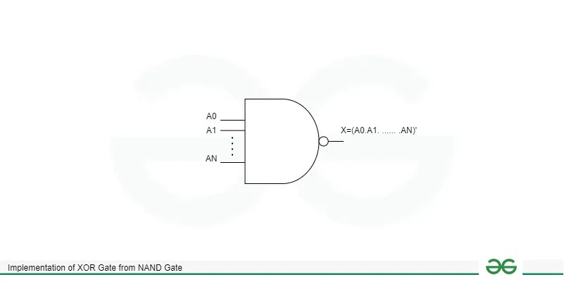 N Input NAND Gate Implementation of XOR Gate from NAND GateExpression of XOR gate: A’.B + A.B’ To convert the expression into NAND form perform the following:
Pass Input A through the first NAND Gate to get A’, now pass this A’ and B through the second NAND Gate to get (A’.B)’. Similarly, pass Input B through the third NAND Gate to get B’, now pass this B’ and A through the fourth NAND Gate to get (A.B’)’. Pass both the output (A’.B)’ and (A.B’)’ through the fifth NAND Gate to get our desired expression of XOR Gate ((A’.B)’.(A.B’)’)’ = A’B + AB’ (By De-Morgans Law). Logic diagramThe Logical Diagram of the Following Expression is shown below 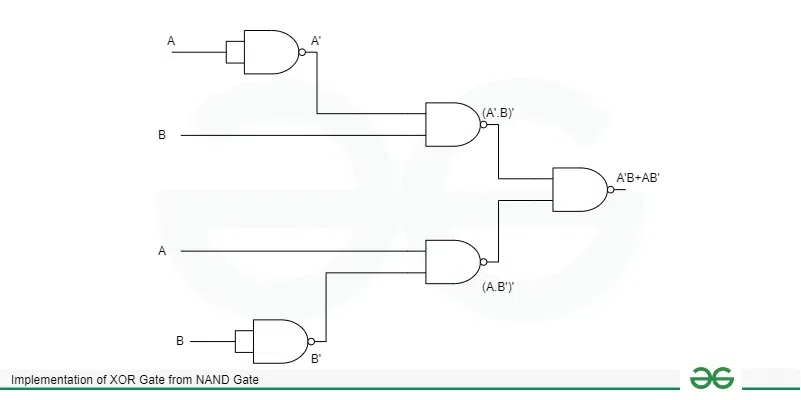 XOR Gate from NAND Gate ConclusionThe use of NAND Gates to achieve the logical XOR operations demonstrates the efficiency, usability and adaptability of NAND Gates in simplifying circuit design and also provides valuable insights into the fundamental principles of digital electronics. With just five NAND gates, we can construct XOR gate. This process also involves the application of De Morgan’s law to convert the expressions. It shows how a logic function can be simplified using universal gates, reducing the complexity and cost. Implementation of XOR Gate from NAND Gate – FAQsWhat are Universal Gates?
What are Fundamental Gates?
How is a NAND gate different from an AND gate?
|
Reffered: https://www.geeksforgeeks.org
| Analog And Digital Electronics |
Type: | Geek |
Category: | Coding |
Sub Category: | Tutorial |
Uploaded by: | Admin |
Views: | 15 |