
|
|
The term “transistor” originated in 1951 at Bell Laboratories by Dr. Shockley and associates. The transistor is a widely utilized essential component in modern electronic systems. Transistors generally come in two types. They are field effect transistor (FET) and BJT which is bipolar junction transistor. Signal amplification, or amplifier usage, is a common use of a BJT ( bipolar junction transistor), which is a three-terminal semiconductor device composed of combinations of p-type and n-type semiconductors. As we know this semiconductor device consists of the p-n junction and it is used or able to amplify the signal or magnify the signal. Through this the current flows and basically it contains silicon, they are also called bias resistor built-in transistors and their main objective is that -as the small current flows between the base and emitter which can control a large flow of current between the regions of collector and emitter terminals. Table of Content What is Bipolar Junction Transistor?The concept of BJT refers to a three-terminal semiconductor device consisting of two p-n-junctions that are formed by sandwiching either p-type or n-type semiconductors between two p-type semiconductors. Transistors can be used to transfer input signals through the circuits having lower to higher resistance. A BJT may also be implemented as a true solid-state switch in electrical circuits and can also be used to increase the strength of a weak signal. Symbol of BJT Construction of BJTCombinations of p-n junctions, or build a BJT i.e. a BJT is made of p and n type semiconductors. The two junctions divide the three semiconductors of a BJT which are: the base, collector, and the emitter. The emitter and collector part of transistor are placed on each side of the base.
There are two junctions formed in BJT . They are –
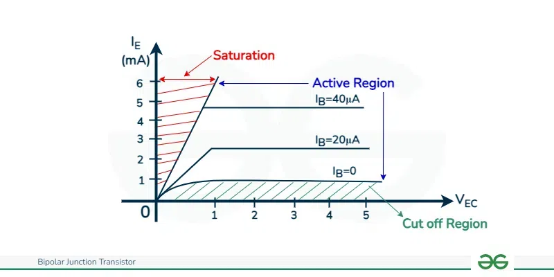
 Construction of BJT Operation of BJTBJT operates in three regions:
 Regions of Operation of BJT Types of BJTsBJT could possibly be divided into two broad groups based on how the p-type and n-type semiconductor materials are arranged physically:
NPN TransistorP-type material is sandwiched between the two n-type of semiconductors in NPN type semiconductor. The two semiconductors of the n type act as the emitter and collector, respectively, while of p-type acts as the base. The Emitter-base junction is forward bias and collector-base is reverse bias during the forward active state of NPN transistor. Only if voltage exceeds the barrier potential, which is 0.3 volts for germanium transistors and 0.7 volts for silicon transistors, is the emitter-base junction forward biased. Due to forward bias on the emitter- base junction the free electrons move towards the base region in N –type emitter. This constitutes emitter current . Direction of conventional current is opposite to the flow of electrons. Electrons after reaching the base region tend to combine with the holes. If these free electron combine with holes in the base, they constitute base current . Most of the free electrons do not combine with the holes in the base as base and the width is made extremely small and electrons do not get sufficient holes for recombination. Thus most of the electrons will diffuse to the collector region and constitutes collector current . There is another component of collector current due to the thermal generated carriers. known as reverse saturation current and is quite small.  NPN BJT PNP TransistorThe two p-type of semiconductors are sandwiched between the n-type semiconductor in a PNP BJT. The two p-type semiconductors act as the emitter and collector, respectively, and the n-type acts as the base. In a PNP transistor, current is due to the movement of holes, as opposed to the mobility of free electrons in an NPN transistor. The collector base junction of a PNP transistor is reverse biased, whereas the emitter base junction is biased forward. The holes within the emitter area flow into the base region due to the forward bias at the emitter-base junction. This constitutes the emitter current . The holes after reaching the base region, combine with the electrons in the base and constitutes base current. Most of the holes do not combine with the electrons in the base region as base width is made extremely small, and holes does not get sufficient electrons for recombination. Thus most of the holes diffuse to the collector region and constitutes collector region. There is small component of collector current due to the thermally generated carriers . This is called reverse saturation current.  PNP BJT The transistor is fundamentally a current-controlled device, hence the voltage between its terminals has significant effect on its behavior.
Bipolar Transistor ConfigurationsThere are basically three possible ways to connect BJT in an electric circuit are:
Common Base ConfigurationThe base of transistor is grounded in common base characteristics , with the emitter acting as the input and the collector as the output. The emitter-base junction is biased forward, whereas the junction between the collector and the base is reverse biased. Low voltage gain but high current gain is offered by the CB arrangement. It is frequently employed in impedance matching. It reverses the output signal’s phase with respect to the input and frequently utilized as a buffer between circuits with high and low impedance and in high-frequency applications like RF amplifiers. Characteristics curvesThere are two important characteristics of a transistor.
 Input characteristics
.png) Output characteristics Common Emitter ConfigurationEmitter of transistor is grounded in common-emitter characteristics , and the base serves as input and the collector serves as output. The CE configuration is like the CB configuration, it has a forward biased BE junction and a reverse biased CB junction. The voltages of CB and CE configurations are related by:
and the emitter current in given by :
A CE design offers a modest current gain together with a strong voltage gain. It is frequently employed in voltage amplification. In a Phase Relationship, it Flips the phase of input signal in relation to the output. Typically used in general-purpose amplification, audio amplifiers and RF amplifiers . Characteristics curves
 Input Characteristics
 Output Characteristics Common Collector ConfigurationIn the common collector characteristics, the collector of the transistor is grounded, then the base turns as input and the emitter turns as output. One voltage gain but a significant current gain is achieved with the CC setup. It serves mostly as a buffer for current. Phase Relationship: Preserves the identical phase between the signals received and sent. It include impedance transformation, impedance buffering, and voltage following to match impedance between circuits. Characteristics curves
 Input Characteristics
 Output Characteristics
Functions of BJTThe most well- known functions of BJT are :
Advantages of BJTFew advantages of BJT includes :
Disadvantages of BJTFew disadvantages of BJT includes :
Applications of BJTSome of the well – known applications of BJT includes-
ConclusionIts a key component for amplification , therefore making it an essential element in the field of electronics. It can operate circuits , enhance signals ,works as switch . The BJT has three layer structure – emitter , base , and the collector which allows it to operate in various configurations . The simplicity , detailed concepts, reliability makes it an important component in electronic circuits. It is the foundation for more complex circuits. So the main aim is to amplify or switch the power and as it can operate in three regions which enable them to act as an amplifier or switch, which does not need to carry any external source for amplification process. FAQs on BJTWhat’s the consequences of not biasing a transistor properly ?
Can the sides of emitter and collector in BJT be changed.
Which type of transistor is fast ?
|
Reffered: https://www.geeksforgeeks.org
| Electronic Devices |
Type: | Geek |
Category: | Coding |
Sub Category: | Tutorial |
Uploaded by: | Admin |
Views: | 11 |