|
|
Forward Bias is a term commonly used in semiconductor electronics, particularly concerning diodes and transistors. A diode is considered to be in forward bias when its p-side is connected to the positive side of a power supply and its n-side to the negative side. In the case of an NPN transistor, the base-emitter junction is forward-biased, which means the base is positive relative to the emitter. Conversely, for a PNP transistor, the base is negative relative to the emitter. In this article, we will discuss all Forward Biases including Forward Bias of PN junctions and transistors. Table of Content What Is Forward Biasing?Forward bias refers to a condition in electronics where a positive voltage is applied to the p-type material (anode) and a negative voltage to the n-type material (cathode) of a semiconductor device like a diode. This setup reduces the width of the depletion region at the p-n junction, which is a region devoid of free carriers (electrons and holes) and acts as a barrier to current flow in the diode. In forward bias, the applied voltage essentially narrows this depletion zone and lowers the barrier, allowing charge carriers to cross the junction. As a result, electrons can move from the n-type material to the p-type material, and holes can move in the opposite direction, allowing electric current to flow through the device. Forward Bias Definition
In simple words, we can say forward bias is a condition in which the voltage applied to a semiconductor diode allows current to flow easily through the diode. Effects of Forward BiasingThe following sequence of events happens in a forward biased junction diode.
Forward Biasing CharactersticsThe characteristics of a diode under forward bias:
In forward bias, the positive terminal of the voltage source is connected to the p-type (positive) semiconductor material, and the negative terminal is connected to the n-type (negative) semiconductor material. This arrangement reduces the potential barrier at the junction, allowing charge carriers (electrons in the n-type material and holes in the p-type material) to move across the junction more easily.
The forward bias reduces the potential barrier at the p-n junction. This barrier is essentially the energy barrier that prevents the flow of majority carriers across the junction.As the forward voltage is increased, the barrier potential decreases.
With the reduced barrier potential, charge carriers can overcome the potential barrier and move across the junction.Current starts to flow through the diode in the direction of the external voltage.
Under forward bias, the diode exhibits low resistance, allowing for efficient conduction of current.
The forward voltage drop (Vf) is the voltage at which the diode starts conducting significantly. This voltage varies depending on the type of diode (e.g., silicon diodes typically have a forward voltage drop of around 0.7 volts). What is P-N Junction Diode?A P-N junction diode is a two-electrode semiconductor where the electric current flows only in one direction. The device does not allow the electric current to flow in the opposite direction. If a P-N junction diode facilitates the flow of electric current when the applied voltage is present, it is a forward bias P-N junction diode. Different types of semiconductor materials, such as silicon, gallium arsenide, and germanium, are used to construct P-N junction diodes. Read More about P-N Junction Diode. Forward Bias P-N Junction Diode
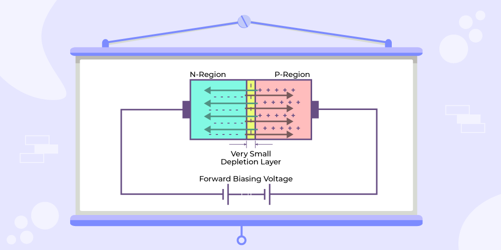
When any type of P-N junction is in forward bias, a resistor Rs must be connected in series with the diode.The function of the limiting resistance is to limit the forward current into the diode. Under forward bias the field of the space charge region and forward voltage Vd will oppose each other. Hence, the resultant electric field is very small, and it is experimentally found that the field is always directed from N to P.When the P-N junction is forward bias, the barrier height reduces by |V0|(magnitude of VD). Circuit Diagram of Forward Bias P-N JunctionThe following is the illustration for circuit diagram of forward bias P-N Junction:
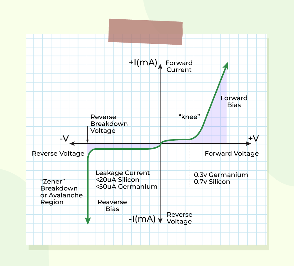
IV Curve For Forward Bias P-N Junction DiodeIn forward biasing, forward current flows in the circuit. When the forward voltage equals zero, the value of forward current is also 0 mA. There is an increase in the current in forward bias diodes with increase in forward voltage till the point known as knee voltage. Beyond this point, the forward current increases rapidly.
Learn more about: IV Characterstics of PN Junction Diode. Different Cases of Forward BiasThere are three cases for
Barrier voltage (V0) is dominating. Hence, no majority carrier will be crossing the junction.
In this case, since the forward voltage of the diode which means more majority carriers will be able to cross the junction, and the forward current increases exponentially with the forward voltage VD. The diode is now in a conducting state, or the diode is in the ON state.
The effect of the barrier is nullified, i.e., the barrier will no longer oppose any majority carriers crossing the junction. Both the majority and minority carriers will be able to cross the junction. Hence, the forward current is small, or it just starts to flow into the diode. Forward Current EquationThe diode current equation shows the relationship between the current flowing through the diode as a function of applied voltage. The mathematical expression of the diode current is given below.
Where,
Forward and Reverse BiasAs we already discussed that, in forward biasing the external voltage is applied across the PN-junction diode. This voltage cancels the potential barrier and provides the low resistance path to the flow of current. In reversed bias the negative region is connected to the positive terminal of the battery and the positive region is connected to the negative terminal. The reverse potential increases the strength of the potential barrier. The potential barrier resists the flow of charge carrier across the junction. It creates a high resistive path in which no current flows through the circuit. Difference between Forward and Reverse BiasThe key differences between both forward and reverse bias are:
Applications of Forward BiasSome of the most common appliactions of forward bias are:
Conclusion: Forward BiasIn conclusion, forward biasing is a fundamental principle in semiconductor devices, particularly diodes, and plays a vital role in enabling the controlled flow of current through electronic circuits. Understanding the behavior of diodes under forward bias is essential for designing and analyzing electronic systems. Read More, Frequently Asked Questions on Forward BiasDefine Forward Bias.
What is Reverse Bias?
What are the Characteristics of Forward Bias?
Which Instrument are Operated on the Principle of Forward Bias?
Which of the Junction Diode is Used in Forwaed Bias?
|
|||||||||||||||||||||||||||||||||
Reffered: https://www.geeksforgeeks.org
| Class 12 |
Type: | Geek |
Category: | Coding |
Sub Category: | Tutorial |
Uploaded by: | Admin |
Views: | 13 |